New solution for three-dimensional integration of semiconductor devices
Aerosol Jet Printing for heterogeneous 3D integration in semiconductor modules
Miniaturisation in the 3rd dimension - form factor opens up new markets
Miniaturisation has gained outstanding importance in modern semiconductor technology.
In addition, there is the increased mobility of the end devices - especially with mobile electronics, the form factor plays an increasingly prominent role.
The goal of the semiconductor industry is therefore to integrate performance within the smallest volumes.
In this respect, the process leads from 2D to 3D integration. This involves stacking components in the third dimension. This is achieved by stacking different components on top of each other within a single enclosure. The classic printed circuit board with the semiconductor components located next to each other can thus be integrated into a single housing (chip). Various individual components (dies) are then placed on top of each other on this chip.
The technological requirements for such 3D integration are very high and industrial manufacturing standards must be implemented in the solution. This is where the new process for the three-dimensional integration of semiconductor components offers an innovative solution.
State of technology & the future
Status quo:
Already today, semiconductor components are assembled into stacks.
The challenge:
- Connection - how to connect the different stacked components electrically.
- Heterogeneity - the higher the number and the more varied the geometric and circuit design of the stacked components, the more difficult stacking becomes.
Procedures to date:
Wire bonding:
Wire bonding was initially used to make electrical contact between the components of a stack.
Disadvantages of this process:
- The requirements, such as radii of curvature and accessibility to the contact surfaces, set clear limits.
- The electrical contacting can generate disturbing electrical fields or electrical fields can disturb the contacting.
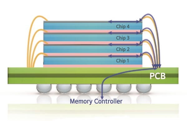
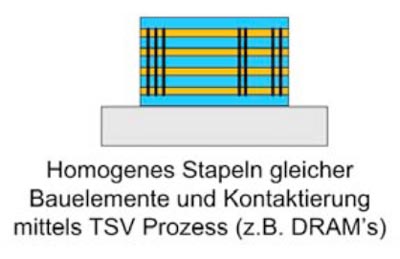
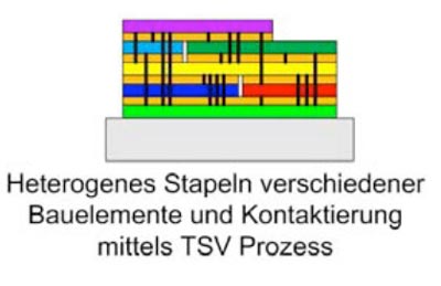
TSV (Through-Silicon-Via) technology:
In this process, small openings (vias) are etched into the thin wafer using a deep-etch process (e.g. BOSCH process). These are subsequently filled with metal. With this method, it is now possible to lead an electrical contact from the front side of a wafer to its rear side in an extremely short path.
Disadvantages of this process:
- The geometric placement of the contact points is complex.
- This method is often not suitable for heterogeneous stacks.
- Thermal management is challenging sometimes.
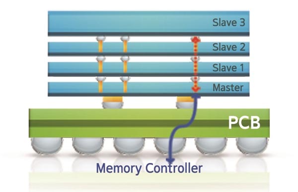
Si or glass interposer:
Currently, Si or glass interposers are used for rewiring stacked wafers. In this way, contact points can be geometrically relocated or supplemented using lithographically applied conductor tracks.
Disadvantages of this process:
- Lithographic processes are costly.
- Lithographic processes are inflexible.
- Time-to-market is high due to the effort involved.
- Heterogeneous stacks - stacks of several different components in unequal geometrical layout are difficult to wire.
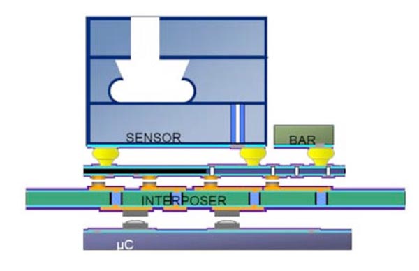
Printed interposer - revolution in the integration of semiconductor components
The principle of 3D printed interposers
Wiring is printed on the surfaces of the semiconductor components.
By using this new type of printed wiring, memory elements can be stacked very easily.
Advantages: This process can be done within a single plant and involves low material costs only.
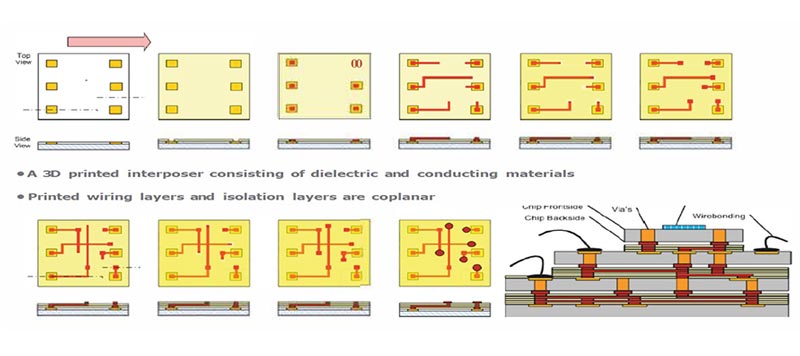
Printed interposer - breakthrough innovation
Wiring is printed onto the surfaces of the semiconductor components using metal-enriched nano inks. Subsequently, the components can be stacked very easily - similar to storage elements.
Advantages:
- As it is a 3D printing process, conductive traces can be easily crossed and contact points can be adjusted as desired.
- This process can be done within a single plant and involves low material costs only.
Advantages of printed interposers
Unfavourably positioned contact points of a semiconductor component are moved by printed structures so that they are in the ideal position before stacking.
Advantages:
- For the first time, it is possible to stack heterogeneous wavers almost as desired.
- The high flexibility of the printing process means that changes can be carried out quickly and easily - minimising development costs and time.
Technological requirements for printed interposers
It is only through the availability of two innovative technologies that it has become possible to print interposers:
- Aerosol continuous jet printer
- Metallic nano-particle inks
Today already, passive components are being printed successfully, which means that empirical values are available. A number of companies have specialised in such printing processes and inks.
Advantages compared to current technologies
Flexibility
Electrically conductive structures and sensors in the micrometre range can be effectively manufactured.
Bypassing the Known Good Die (KGD)
Picking of defect-free components can be done before stacking. This significantly reduces scrap.
Extremely short time-to-market.
Printed interposers can be produced ad hoc in a single print run using the appropriate software.
Customisation by software
CAD files can be read in directly and the structures printed accordingly. This enables a simple and fast transfer from design to printed structure. Developers and designers can therefore develop new types of products quicker and thus contribute to cost reduction and quality optimisation.
Lower material costs
Since the Aerosol Jet® Printing process causes hardly any material waste and material savings can already be considered in the design, this has a positive effect on the environmental and cost balance. The process therefore makes a substantial contribution to minimising the consumption of resources.
Lower investment costs
The investment costs of the lithographic processes used so far are about three times as high as the investment costs for the Aerosol Jet® Printing process. Compared to the lithographic process, the new method enables a fast-structured application on wafers using a few process steps only.
What experts say about 3D integration using aerosol jet printing

Fraunhofer Institute for Electronic Nano Systems ENAS
Chemnitz and Paderborn 2021
Tobias Seifert, Frank Roscher
The number of applications in which printing processes are used for electrical contacting is increasing constantly. There are several reasons for this:
- In recent years, the quality of printable materials has been significantly improved.
- The variety of materials has been considerably increased.
- The reliability has been substantially improved.
Conclusion: In future, a steady growth of printing processes in the production of electronic systems can be expected. Digital printing processes such as the aerosol jet printing process can be used in the field of packaging as a substitute for wire bonding processes (e.g. for standard MMIC components).
In particular, digital design aspects and fast implementation possibilities for prototypes benefit from this process.
In general, the application of printed RDLs according to the current state of technology is not only expected to have application potential in the prototyping area or low-performance area. Series production is also conceivable for each product class with a fully qualified and optimised process chain including a service life analysis.

Dresden University of Technology
Faculty of Electrical Engineering and Information Technology 2021
Professor Dr Ing. habil. Jens Lienig, Dr Ing. Frank Reifegerste
The technology report on the process "Aerosol Jet Printing for heterogeneous 3D integration in semiconductor modules" summarises the advantages as follows:
- The integration of different elements in one package is a unique selling point.
- For the first time, the integration of sensors, MEMS, chemical components (lab on chip), micro actuators, photonic components (radiation, colour, light sensors, solar cells, LED, laser), other semiconductors (III/IV semiconductors, SiC, SiGe) as well as RF components (waveguides, antennas) has become possible.
- In medical technology, aerosol jet printing can be used to produce components in a highly miniaturised device system.
- IoT - heterogeneous 3D integration using aerosol jet printing can demonstrate its advantages in sensor networks in environmental measurement technology (water and air quality, heating, ventilation, lighting controls, greenhouse controls), applications in the energy industry (condition monitoring of wind turbines and overhead lines) or in building monitoring (measurement of moisture, strain, temperature).
- In the consumer sector, possible applications are conceivable, for example, in the measurement of bodily functions in athletes.

Fraunhofer Institute for Manufacturing Technology and Applied Material Research
Bremen 2021
Timo Rusch, Dr. Ingo Wirth
The report of the Fraunhofer Institute on the Aerosol Jet® Printing process for use in semiconductor manufacturing comes to the following conclusion:
- Although Aerosol Jet® Printing has already been used in many areas, this process has hardly been used in the field of manufacturing in the semiconductor industry so far, despite many advantages - established lithographic processes are still relied upon.
- While the lithographic process is a high-volume process, the Aerosol Jet® process, as a CAD-supported additive manufacturing process, offers the greatest possible flexibility and significant economic advantages as well as a lower process cost compared to the lithographic process.
- The material waste associated with conventional subtractive processes can be avoided by using the Aerosol Jet® process. As material is only applied to the previously determined areas, the process is resource-efficient and sustainable (Hedges, 2005).
Advantages:
- Aerosol Jet® Printing can be used to coat wafers and other planar, curved or complexly shaped surfaces with a resolution of up to 10 μm.
- Small structures in particular can be applied quickly and economically without masks.
- The printing process offers great advantages for multilayer structures, for example in the production of interposer layers.
Comparison of Si or glass interposers versus printed interposers
Lihographically produced interposer |
Printed interposer |
|
 |
 |
|
|
Size of structure |
any size smal |
5-20 um |
|
Wiring layers |
2 maximum |
any desired |
|
Passive components |
Yes |
Yes |
|
Contacting by |
Bumps |
Bumps |
|
Thickness of the interposer |
approx. 50 µ |
5-30 µ |
|
Interposer on wafer level |
Yes |
Yes |
|
Interposer on die level |
No |
Yes |
|
Production costs of Interposer |
high to very high |
low (single-step process) |
|
Material costs |
high (Si wafer) |
low |
|
Adjustment |
difficult |
very easy |
|
Costs |
high |
low |
|
Heat dissipation |
by bumps only |
full surface on one side |
|
Complex heterogeneous stacks |
difficult to impossible |
very easy |
|
Challenges |
Complexity, costs and effort |
Optimisation of the printing process |
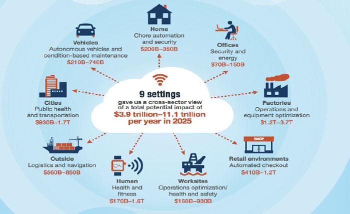
Future market - Internet of Things (IoT) & bioelectronics
The wide range of applications for printed interposers opens up a huge market volume.
Markets of the future include:
-
IoT (internet of things)
-
Bioelectronics
-
Safety and energy sector
-
Automotive industry
-
Public health services
-
Logistics and navigation systems
-
Automation and monitoring in production
-
Smarthome